Introduction
ThinkPad X61 is a classical machine, along with T61 they are the last 4:3 ThinkPads made by Lenovo. I bought my X61s used in 2010 (I simply couldn't afford it back in 2007 when it first came out) and keeps using it as my main laptop (I have a much more powerful desktop PC for most of the stuff though). Many of the components have been upgraded since then, 2GB DDR2 is upgraded to 6GB, 160GB spin drive has been replaced by a 512GB SSD, and the TN screen has been replaced with an AFFS (IPS) screen. The thing that never changed is the processor: the 65nm Core 2 Duo L7500.
X61 comes with various CPU options available when buying new:
X61:
- Core 2 Duo T7100, 1.8 GHz, 2 MB L2, FSB 800, 65 nm, 35 W
- Core 2 Duo T7250, 2.0 GHz, 2 MB L2, FSB 800, 65 nm, 35 W
- Core 2 Duo T7300, 2.0 GHz, 4 MB L2, FSB 800, 65 nm, 35 W
- Core 2 Duo T8100, 2.1 GHz, 3 MB L2, FSB 800, 45 nm, 35 W
- Core 2 Duo T8300, 2.4 GHz, 3 MB L2, FSB 800, 45 nm, 35 W
- Core 2 Duo T9300, 2.5 GHz, 6 MB L2, FSB 800, 45 nm, 35 W
X61s:
- Core 2 Duo L7300, 1.4 GHz, 4 MB L2, FSB 800, 65 nm, 17 W
- Core 2 Duo L7500, 1.6 GHz, 4 MB L2, FSB 800, 65 nm, 17 W
- Core 2 Duo L7700, 1.8 GHz, 4 MB L2, FSB 800, 65 nm, 17 W
However, when buying used, especially in 2020, it is really hard to pick one specific processor. Most of the listings online come with a T7100 or T7300 processor, built with a 65 nm process. If the machine is an X61s, then the 65 nm processor is pretty much the only choice.
Unless the processor can be replaced or upgraded.
It is quite common to replace the processor in T61s, just buy a new processor, install that on to the motherboard, done. Or if one wants to use newer FSB 1066 processors or even quad-core processor, BIOS mod and motherboard mod are available to allow the processor to run on the T61 motherboard.
The X61, on the other hand, has the processor soldered down on to the board, making it harder to replace the processor. And it is much harder to buy BGA processors than just normal PGA processors: pretty much no one would take out the BGA processor from their laptop and just sell that, and it is pretty hard to buy new old stock BGA processors. But the good thing is if the CPU can be indeed bought and installed, all the mods available to the T61 are also available to the X61.
This post is a comprehensive note about how to install probably any Core 2 Duo mobile processors onto X61 if the power supply and cooling allow. And my method uses a PGA processor rather than a BGA processor so the processor is still easily purchasable on eBay or other platforms. Quad-core processors run much hotter and require further ACPI mod which is not described in this post.
I understand that these kinds of mod have been done on X61 many times before. But I just want to document comprehensively how I did it and what each step is.
I am also aware of the existence of the X62/X63 motherboard project. This project only focuses on upgrading the original motherboard.
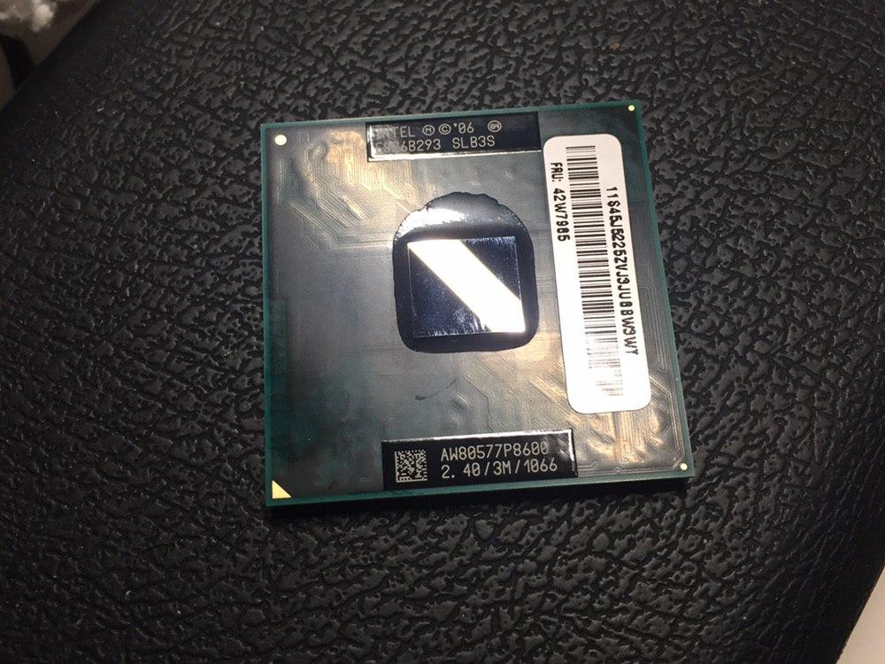
I used P8600 as an example in this post, but other processors should also work.
All information is provided "as is". I will not be responsible for any damage due to the use or misuse of the information provided. Modding BIOS and hardware is risky and likely to permanently brick the machine if not done properly. Do this at your own risk.
What You Need
- An X61 or X61s to be modded
- A Merom or Penryn Socket P processor
- A Windows PC with MinGW/MSYS or a Linux PC with wine, for BIOS modding
- A non-ThinkPad DDR2 laptop, for flashing SPD
- Soldering iron
- Soldering wick
- BGA Flux (RMA-223 or similar thing)
- Hot air soldering Station with board preheater and 35mm x 35mm nozzle
- BGA478/479 reballing stencil
- 0.5mm solder balls (other dimensions may also work)
- Reballing station or some board holder that is resistant to heat
- The 479 interposer board, or access to PCB prototyping service
BIOS mod
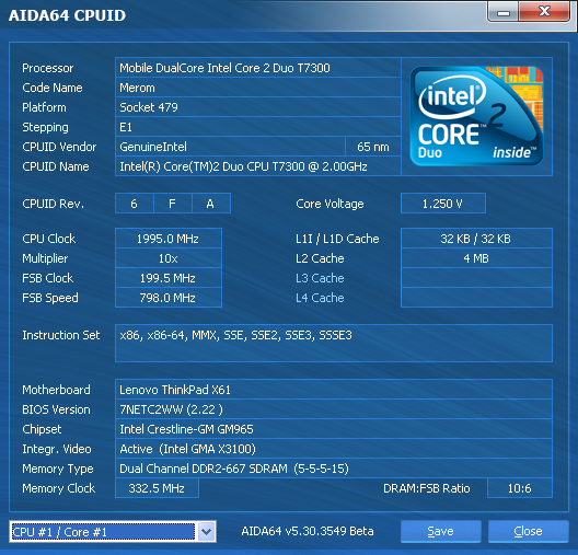
The BIOS needs to have the microcode for the CPU to be installed. The microcode patch binds to the CPUID. In other words, the BIOS needs to have the microcode that matches the CPUID for it to work. If the new CPU can be installed on some other machines to test (for example, maybe a T400), AIDA64 may be used to check the CPUID. Otherwise, the CPUID can be found on http://www.cpu-world.com/CPUs/CPU.html. Processors with the same model number but different stepping may or may not have different CPUIDs.
For example, the CPUID for T7300 is 6FA:
Here are some common ones for reference:
- 6FA: Core 2 Duo L7500, Core 2 Duo T7300
- 6FD: Core 2 Duo U7500, Core 2 Duo T7100
- 10676: Core 2 Duo P8600, Core 2 Duo T9600, Core 2 Extreme X9100
- 1067A: Core 2 Duo P8600, Core 2 Duo P9700, Core 2 Duo T9600, Core 2 Quad Q9100
Generally, to use common T9x00, P8x00, or P9x00 processors, look for 10676 and 1067A.
Note that there are already modded BIOS floating around online.
Check Microcode Patch
This section describes how to check the microcode patch installed in the current BIOS. If the BIOS already has the patch required, then there is no need to further mod the BIOS.
A BIOS dump is necessary for this step. No, the BIOS upgrade downloaded from Lenovo won't work. The dump can be obtained by using phlash16 with the following command:
PHLASH16 /RO=X61BAK.ROM BIOS.WPH
Note that it does require a BIOS upgrade file even if it is only instructed to backup. It doesn't need to be valid though. Somehow WinPlash just simply doesn't work for me, the backup is corrupted. And WinPlash only supports 32-bit OSes which is getting rare, so just might as well make a USB DOS boot disk for the job. Rufus can create FreeDOS or MS-DOS boot disks.
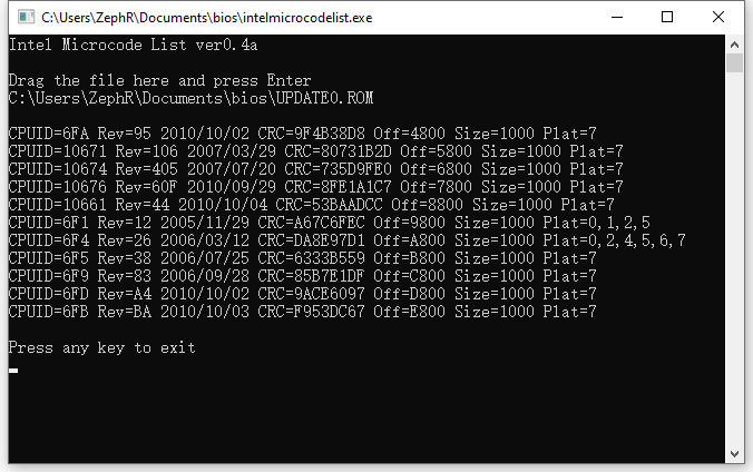
After the step is done, open up the intelmicrocodelist.exe, drag and drop the BIOS dump into the new window, press Enter. It should show all the microcode patch that the BIOS already has.
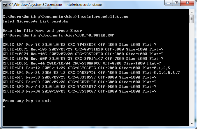
This is the microcode patch that my X61 has. Note it is missing a microcode patch for 1067A, which means some newer stepping of P8x00 or P9x000 won't work. Core 2 Duo E8xxx from iMac also won't work. If the processor happens to be already supported (mostly 10676), then no BIOS-mod is required. Skip to installing the processor.
Get Microcode Update
Method 1: Get from Intel's microcode patch for Linux
First, microcode patches need to be obtained. Before April 2018, one could get the microcode.dat from Intel's website. But since then they have been changing the microcode format. One way to get historical microcode update before April 2018 is to use the version packaged by Linux distributions, for example, Ubuntu:
https://launchpad.net/ubuntu/+source/intel-microcode/3.20180108.0~ubuntu14.04.2
The microcode-yyyymmdd.dat file is the microcode patch. It can be converted to individual binary microcode patches by using microcode.exe:
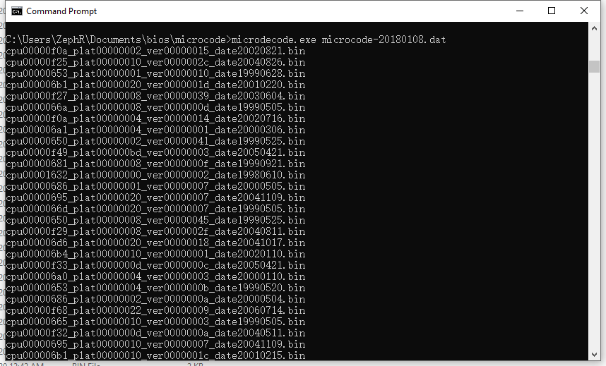
Extract all these files. Now there should be tons of individual .bin files.
Method 2: Extract from BIOS
It is also possible to directly extract microcode patches from a BIOS dump (for example, dump from T400). Use the same intelmicrocodelist.exe, it should tell where all microcode patches are. Use dd to extract them into individual files.
It seems like it contains even newer microcode patches than the Linux patch intel released, I am not sure why.
Extract Microcode Module from BIOS
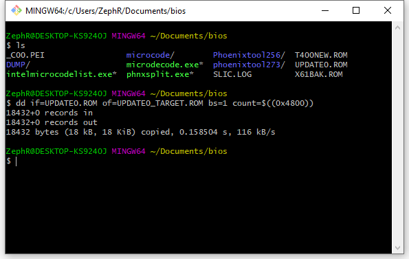
To extract microcode from the BIOS, run the phoenixtool, open the ROM as original ROM. It should extract the ROM automatically and save them to a folder called DUMP.
For X61, UPDATE.ROM contains the microcode patch. This can be verified by using the intelmicrocodelist.exe:
Note the microcode does not start from Offset 0 but ends at the end of the file. This means this file probably contains some other stuff at the beginning of the file, but it should be safe to append more microcodes into the file.
Assemble New Microcode Module
The purpose of this step is to add missing microcode to the X61's UPDATE.ROM.
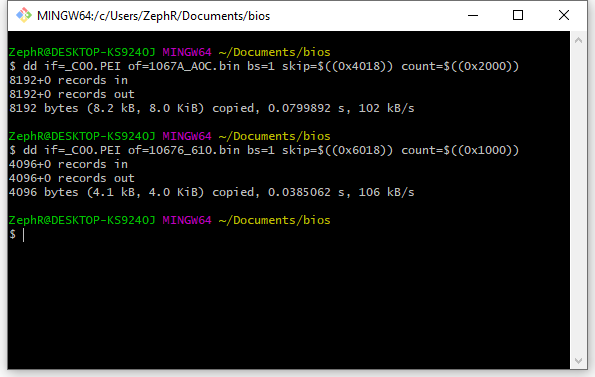
First, extract only the header of the microcode module so later new microcodes can be appended after the header.
Then microcode patches can be appended into the UPDATE0.ROM. I am adding 6FA, 6FD, 10676, and 1067A, which should cover all MP stepping Merom and Penryn processors. However, if the processor is an ES one or an early stepping version, some other microcodes need to be added as well. Simply use the cat command to append it to the end of the new UPDATE0_TARGET.ROM like this:
#!/bin/sh
cat microcode/cpu000006fa_plat00000080_ver00000095_date20101002.bin >> UPDATE0_TARGET.ROM
cat microcode/cpu000006fd_plat00000080_ver000000a4_date20101002.bin >> UPDATE0_TARGET.ROM
cat microcode/cpu00010676_plat00000080_ver0000060f_date20100929.bin >> UPDATE0_TARGET.ROM
cat microcode/cpu0001067a_plat000000a0_ver00000a07_date20080409.bin >> UPDATE0_TARGET.ROM
Done.
Replace the Microcode Module in BIOS
The purpose of this step is to replace the original microcode module in the BIOS with the newly assembled microcode module.
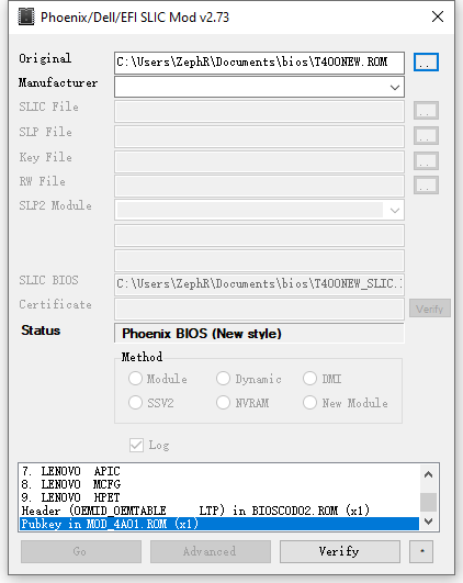
Open the PhoenixTool 2.52 utility. Select the X61 BIOS dump and wait until it unpacks the BIOS. Select Lenovo in the Manufacturer field and click the Advanced button, check "Allow user to modify other modules" and "No SLIC".
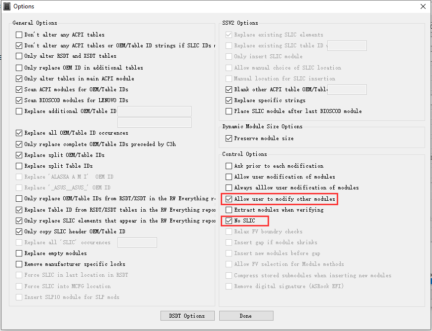
Click "Go". Wait for the prompt to modify the modules.
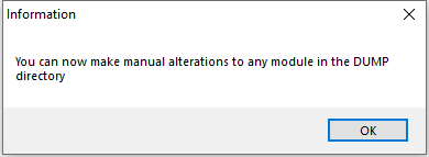
Don't click on OK yet. Go ahead to the DUMP directory, delete the old UPDATE0.ROM and put new UPDATE0.ROM there. Once done, click OK. There should be a new file called X61BAK_SLIC.ROM. You can verify it contains the new microcode patch by, again, using intelmicrocodelist.exe. You can also reopen the ROM with phoenixtool to verify it still contains valid SLIC.
Flash the new BIOS
Copy the new X61BAK_SLIC.ROM to the DOS boot disk. I am calling it X61MOD.ROM.
In DOS, use the following command to update the BIOS:
phlash16.exe X61MOD.ROM /C
Note: /C means invalidate CMOS setting checksum. This forces the new BIOS to reset the CMOS settings. I assume this doesn't matter.
It might warn that the Extended Checksum is not zero. Unfortunately, I don't know how to fix this. For now, simply press Y to ignore the error. Wait for one minute, it should flash the new BIOS successfully.
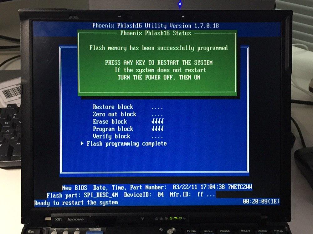
Reboot the machine and hope it still boots. In my case, it does.
Installing the New CPU
Pick a Suitable Processor
Generally, try to use Penryn processors with 6MB L2 cache.
For X61, these machines originally come with 35W processors. One may choose any 35W Core 2 Duo processor, like T9x00. Just keep in mind that processors with high clock speed like T9900 could get quite expensive.
For X61s, the original thermal solution is only designed to handle 17W processors. Unfortunately, the 45nm low power platform used a different set of chipset and processors (GS45 and SU processors) with a different package, so these cannot be used. The next low power choice is the P series processor, which has a TDP of 25W. P8x00 processors come with 3 MB of L2 cache and P9x00 processors come with 6 MB of L2 cache.
I am using a PGA Core 2 Duo P8600 as an example.
Remove Pins on the Processor
PGA processor has metal pins, which are designed to be installed into a socket. However, all the pins on the processor are just soldered on to the processor. It is possible to remove the metal pins with a soldering iron so it can be directly soldered down to the motherboard.
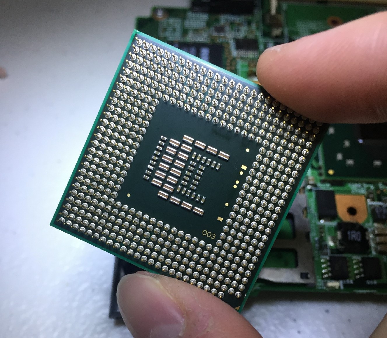
Warning: This step is (obviously) irreversible. You will no longer be able to use this processor in normal Socket P PGA motherboards.
After removing all the pins, remember to use solder wick to clean the solder pads. The right upper corner is cleaned while other areas haven't been cleaned yet.
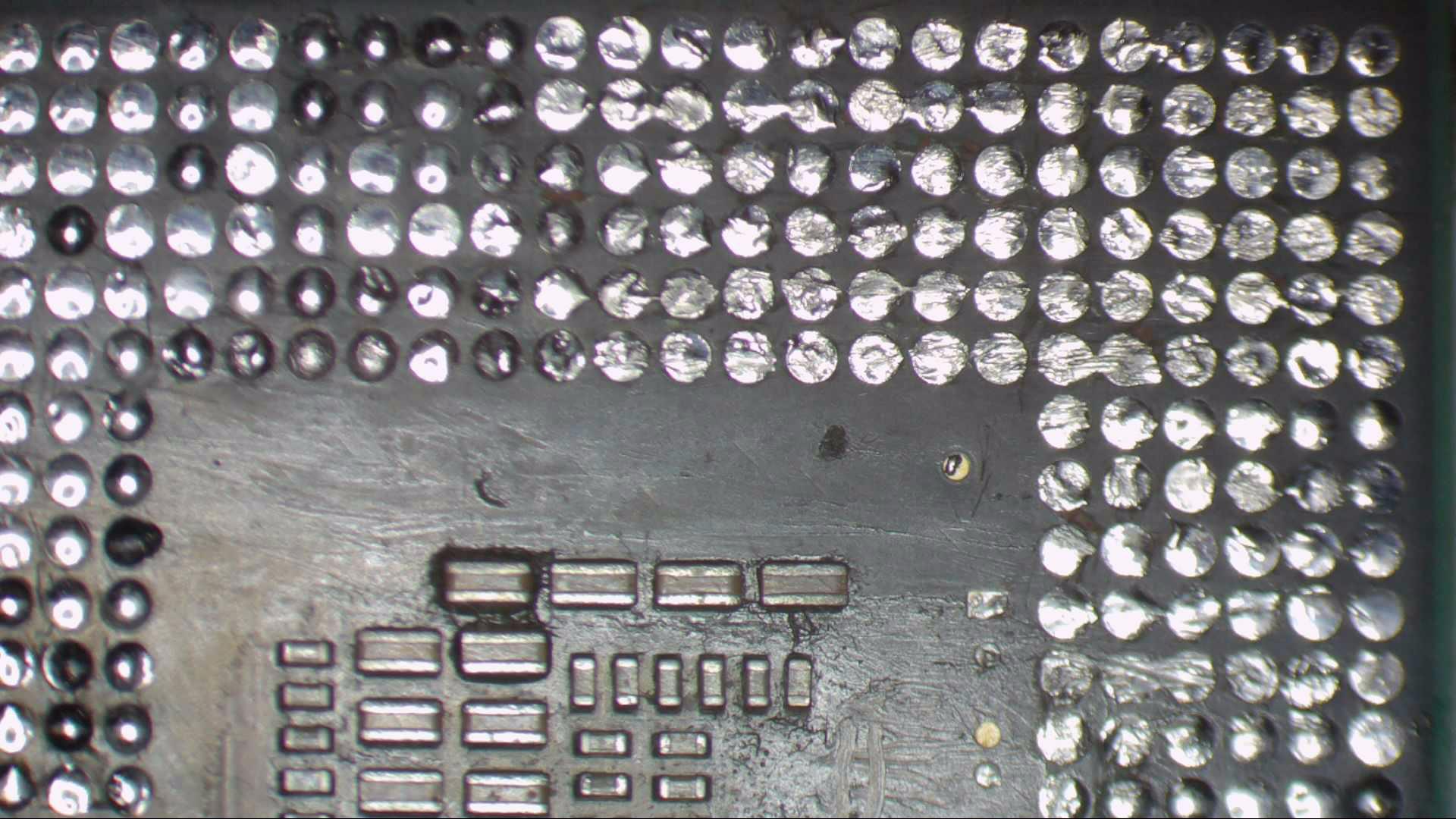
But after removing all the pins, it is still not quite a BGA processor. All the solder pads are larger than that on a real BGA processor. If one is going to reball the processor as if it is a normal BGA processor, the solder balls will melt and become small domes rather than balls. Normally this isn't a big issue. It would only cause the chip to be closer to the board. But this is not the case here. Note there are some capacitors in the center of the processor. These domes are simply not as tall as these capacitors so they cannot make any contact with the board.
There are several potential solutions to this issue:
- Don't remove the pin in the first place. Solder the processor with pin directly on to the motherboard. I doubt if this would work, and this might end up being too thick.
- Use bigger solder balls during the reballing process. 0.76mm balls are known to be too small and that's already the biggest size the stencil will take. But it is still possible to reball it twice.
- Use an interposer board in between the motherboard and the processor. This functions as a stand-off so the capacitors don't touch the motherboard.
I am using the 3rd method. I haven't tested if 1 would work, and I wasn't able to perform 2 without shorting things together.
Interposer Board
The board is nothing more than just directly connecting 478 pins and have a big cut-out in the middle.
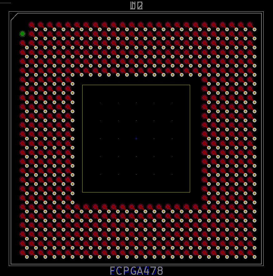
Ideally, the board should be made with a 0.4mm thickness. However, it turns out that 0.4mm boards are much more expensive than 0.6mm boards. As a result, I am using 0.6mm. After receiving the board, plant solder balls on to the board just as if it is a chip except it is double-sided.
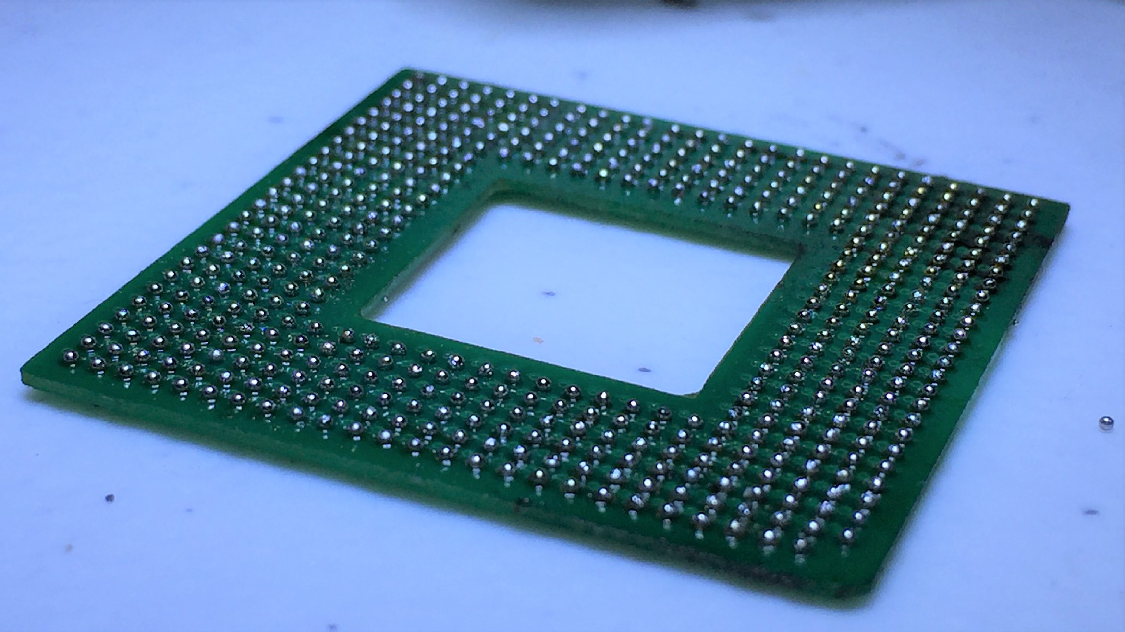
Again, I am planting solder balls on both sides of the interposer board rather than reballing the CPU.
The KiCAD source for the board is available at https://github.com/zephray/Pants479.
Desoldering the Old CPU
Preheat the board to around 140 deg C, heat the chip with 350 - 420 deg C hot air for 1-2 minutes, it should come right off.
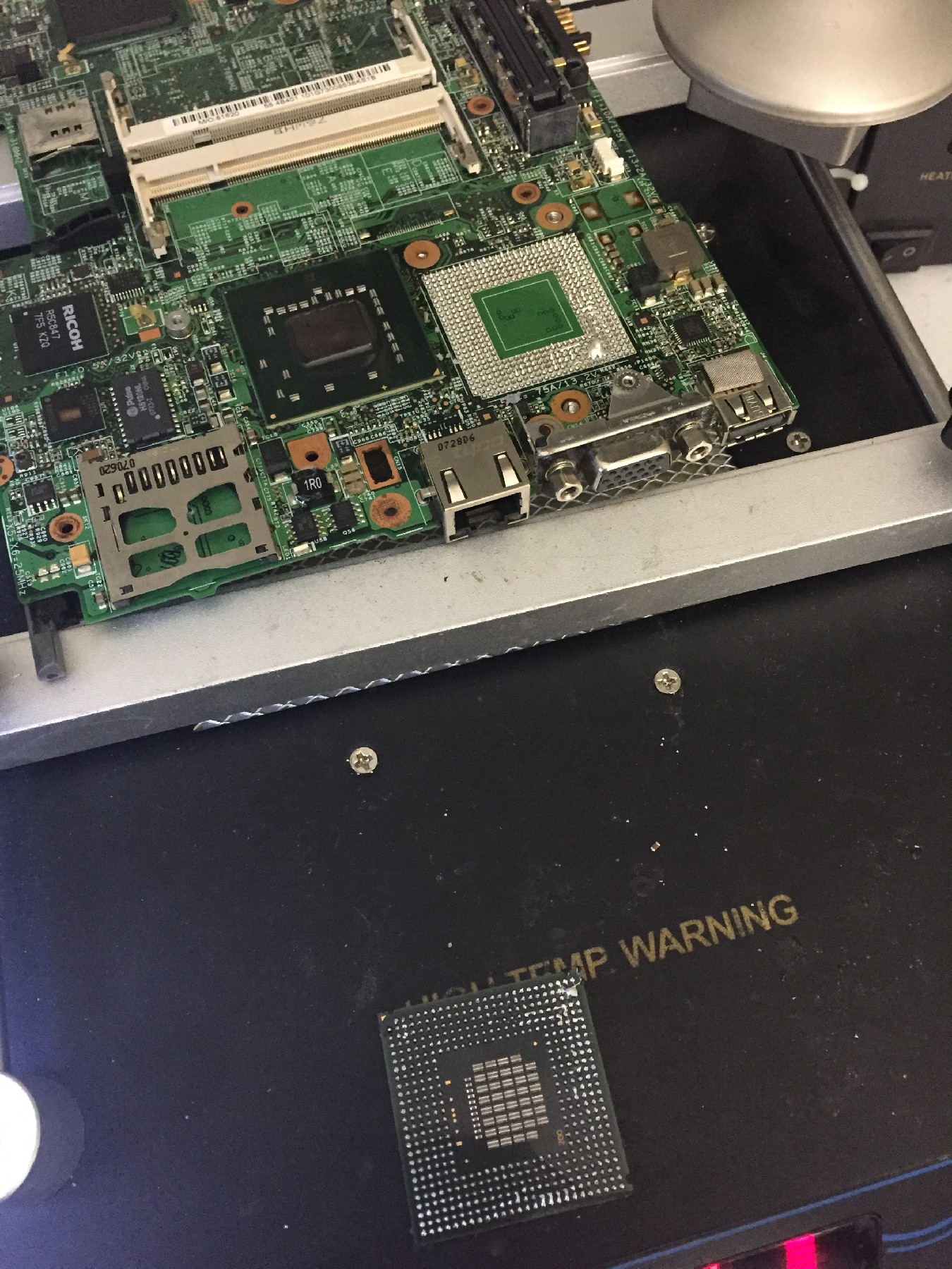
Don't forget to clean the solder pads on the motherboard.
Soldering the New CPU
There is nothing too special about this. Remember to always apply flux to the board. The interposer board needs to be installed on the motherboard first, then the processor can be installed on the interposer board next.
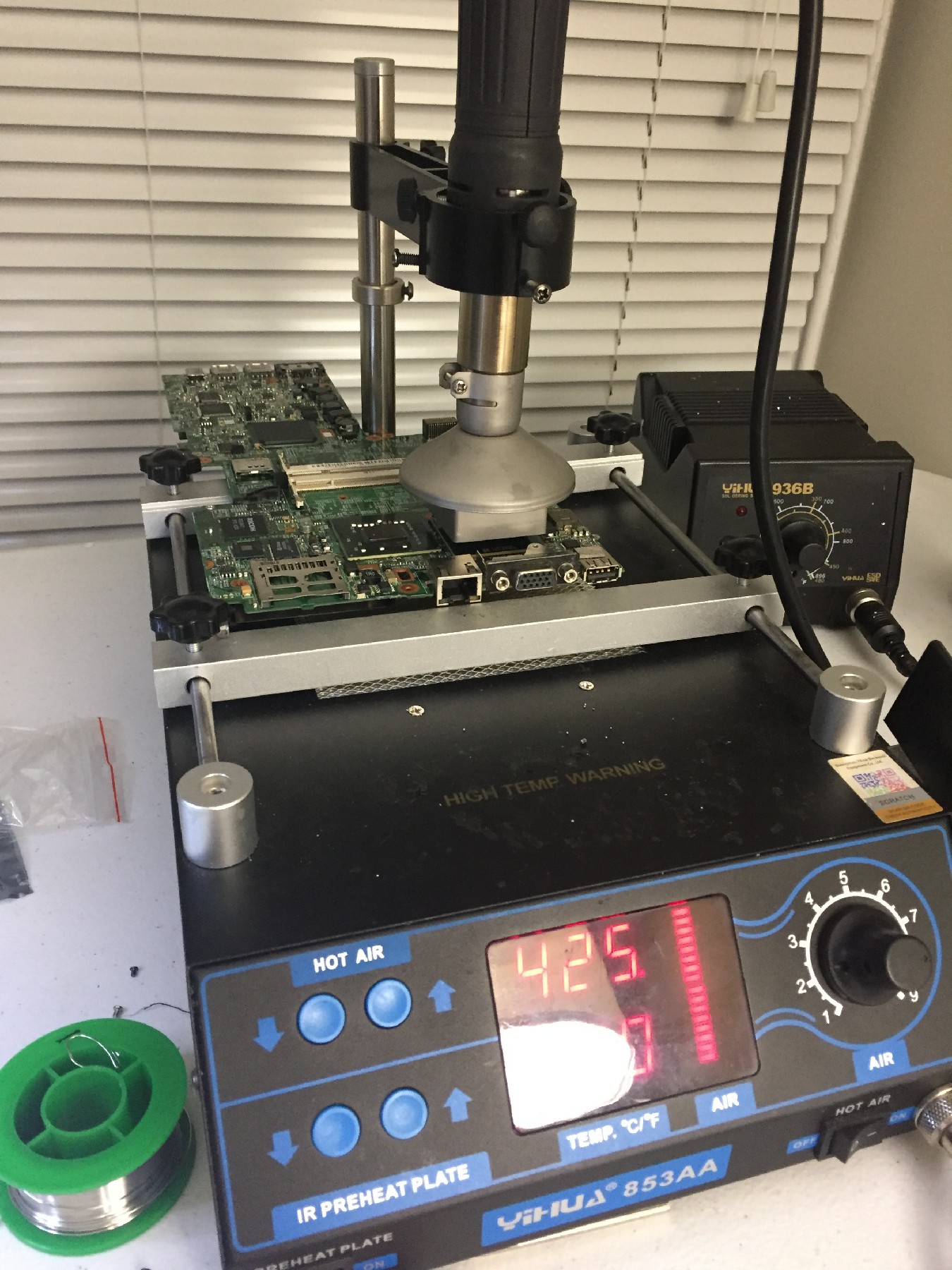
Again, set the preheater to around 140 deg C, 350 degC hot air for 1-2 minutes. If leaded solder balls are used, the temperature can be lower.
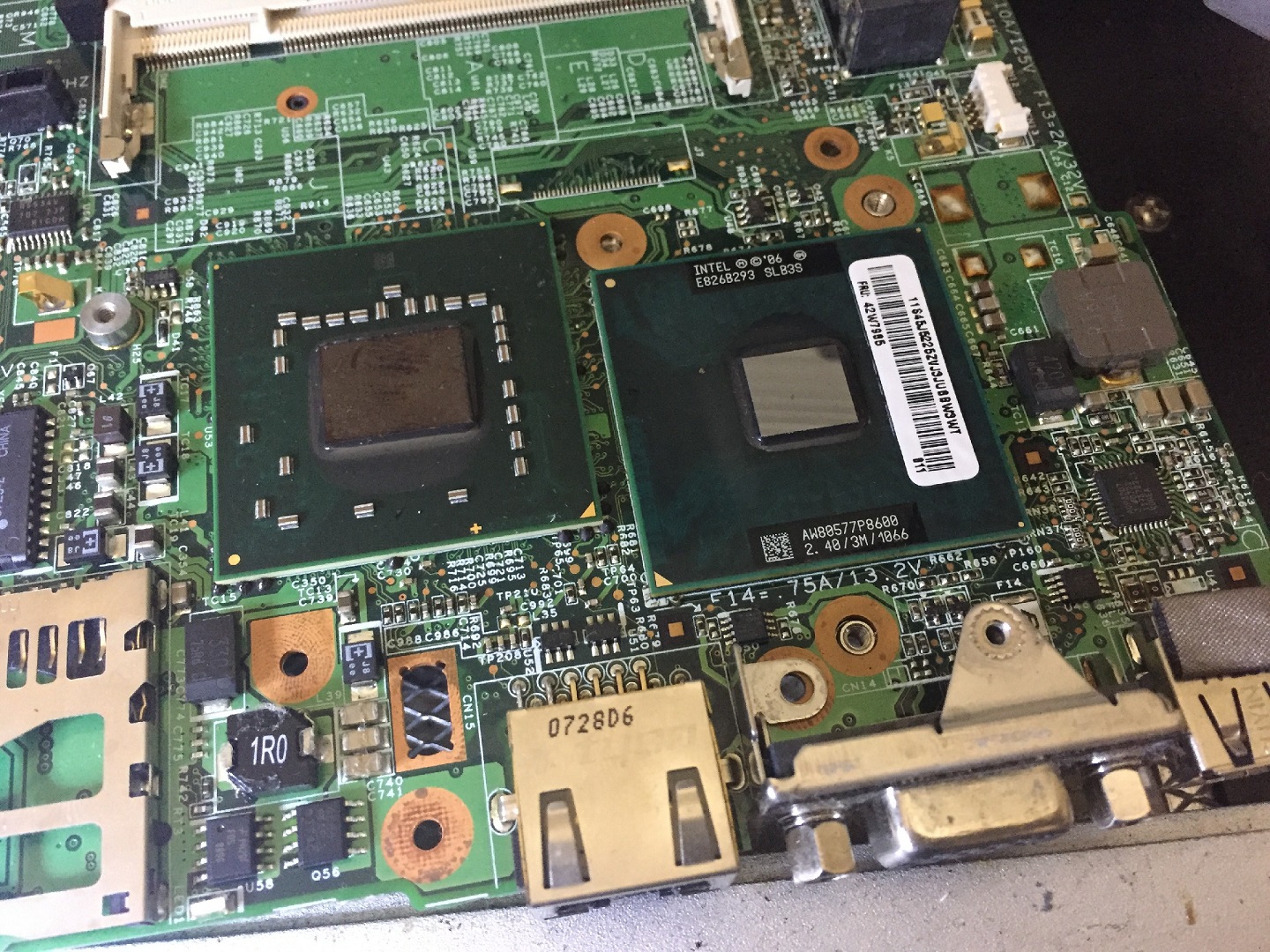
Now the new processor is soldered on the X61 motherboard!
Mod the Motherboard
Unfortunately, at this stage, the motherboard won't boot. To boot an FSB1066 processor on T61/X61, the correct microcode patch is not enough. It will refuse to boot if a 266MHz processor is detected. So the northbridge needs to be tricked into believing a 200MHz processor is installed.
The motherboard detects the base clock of the processor with BSEL pins. On Socket P and Socket LGA775 platforms, there are 3 BSEL lines, with combinations defined below:
| BSEL2 | BSEL1 | BSEL0 | Base Clock |
|---|---|---|---|
| 0 | 0 | 0 | 266 MHz |
| 0 | 0 | 1 | 133 MHz |
| 0 | 1 | 0 | 200 MHz |
| 0 | 1 | 1 | 166 MHz |
| 1 | 0 | 0 | 333 MHz |
| 1 | 0 | 1 | 100 MHz |
| 1 | 1 | 0 | 400 MHz |
| 1 | 1 | 1 | Invalid |
From the table, the motherboard is expecting to see a 010 signal (200MHz) but the processor will provide a 000 signal (266MHz), cause it fails to boot.
The schematics of X61 shows us how these signals are being connected:
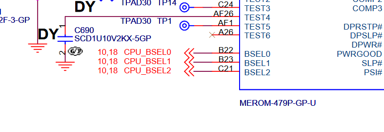
The BSEL signals come from the CPU and go into page 10 and 18.
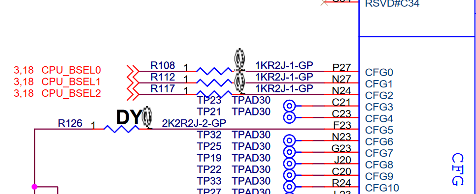
On page 10, these signals go through R108, R112, and R117 and reach the northbridge.
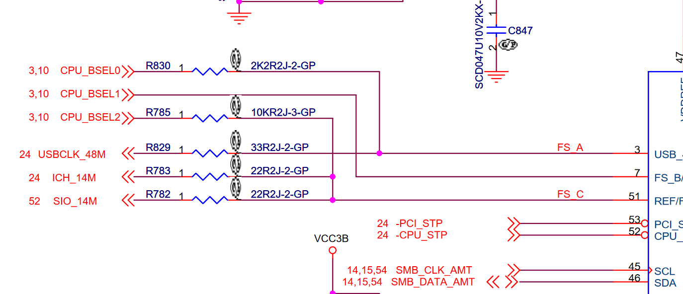
On page 18, these signals go through R830 and R785 and reach the PLL chip (clock synthesizer).
What I want to achieve here is that the northbridge thinks the processor is a 200MHz one, but the clock synthesizer thinks the processor is a 266MHz one. This would allow the system to boot with a 266MHz base clock. To achieve that, the northbridge should receive 010 but the PLL should receive 000.
On to the motherboard, the mod is surprisingly easy: connect these two points with a bodge wire, done. This will pull up the BSEL1 only at the northbridge side.
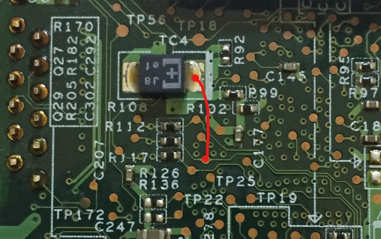
Once this is done, try power it on. There are some chances it may boot up.
Mod the SPD
The reason it may not boot up is that the memory is severely overclocked at this stage. Because the northbridge thinks the base clock is 200MHz, it would configure the clock dividers as if the base clock is 200MHz. But in reality, everything would be 33% higher. For example, if the memory is supposed to run at DDR2-667, it would be running at DDR2-888. Though 888MT/s is not too crazy for DDR2 memories (Some late DDR2 memories can go up to 1066MT/s), but this is under the timing of DDR2-667. For example, many DDR2-667 memory modules have a rated CAS latency of 5, which translates to 1s/667MHz5=7.49ns. On the other hand, many DDR2-800 memory modules have a rated CAS latency of 6, which translates to 1s/800MHz6=7.5ns. Note they are roughly the same: however fast is the transfer rate, the latency shouldn't change. But because the northbridge/BIOS thinks it is running at DDR2-667, it sets the CL to 5. The memory ended up running CL 5 at DDR2-888, translates to an actual CAS Latency of 5.6ns. Not many memory modules can work reliably in such conditions.
The solution is to mod the SPD. The SPD is where all memory timing information is stored. It is possible to mod the SPD so that the memory reports itself as something like DDR2-533 with CL=5. The BIOS would then set the frequency to DDR2-533 and CL to 5. Because the actual frequency is 33% higher, the memory would run at DDR2-708 with CL=5. This is still overclocking the memory, but in practice, this is generally fine.
As this is often done to other machines, I will be brief.
Back up the SPD
Install the memory into a non-ThinkPad DDR2 laptop. ThinkPads disallow accessing the SPD from the OS so they cannot be used. I am using an Asus EeePC for this task.
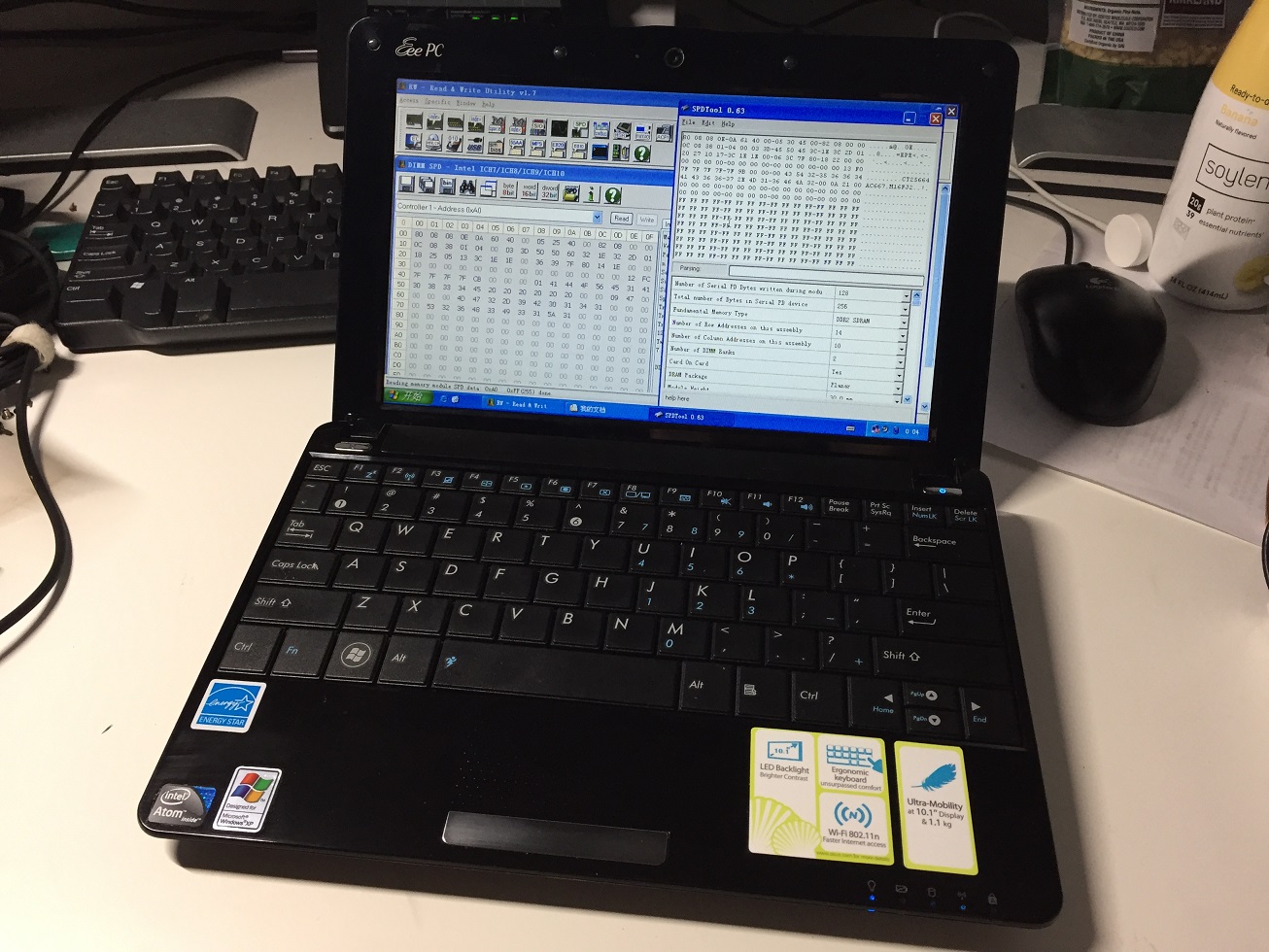
Backup the SPD with software such as RW everything, save it in binary format.
Modifying the SPD
I am using SPDTool 0.63 to modify the SPD. I am setting the timing from DDR2-667 5-5-5-15 to DDR2-533 5-5-5-15 as an example. Generally, this is a good starting point. Change the following properties:
- SDRAM Cycle time at Maximum Supported CAS Latency: 3.75 ns (267 MHz) (from 3.00 ns 333 MHz)
- CAS Latencies Supported: 5 (from 3, 4, 5)
- Minimum Row Precharge Time (tRP): 17.5 ns (from 15 ns)
- Minimum RAS to CAS delay (tRCD): 17.5 ns (from 15 ns)
- Minimum Active to Precharge Time (tRAS): 55 ns (from 45 ns)
Use Edit->Fix Checksum to fix the checksum. Save it as a new SPD file.
Write the SPD Back
RW Everything does not allow write to SPD directly, but it does allow writing to arbitrary SMBus devices, which include the SPD EEPROM. Take a note of the address of the SPD EEPROM, in my case it is 0xA0.
Open up a DIMM SPD editor window, load the modified SPD file, save it as a .rw file. Open the .rw file with a text editor, change the first line from "Type:DIMM SPD Address 00" to "Type:SMBUS Address A0" (replace A0 with your actual address), and delete all the comments in the tail of the file.
Inside RW Everything, click Access->SMBus Device, load the previously modded .rw file, it should automatically write the SPD back to the memory. If you see "SMBus Access Error", this means the SPD EEPROM is write-protected, find another memory module or try to unlock it.
Note that if 2 DIMMs are installed in the X61, the BIOS would always set the timing according to the slower one. So only one of the 2 DIMM needs to be modded.
Done
Finally, done. Try to power on the machine and see if it boots! Note it would always automatically restart the first time if CMOS settings are cleared, this is normal.
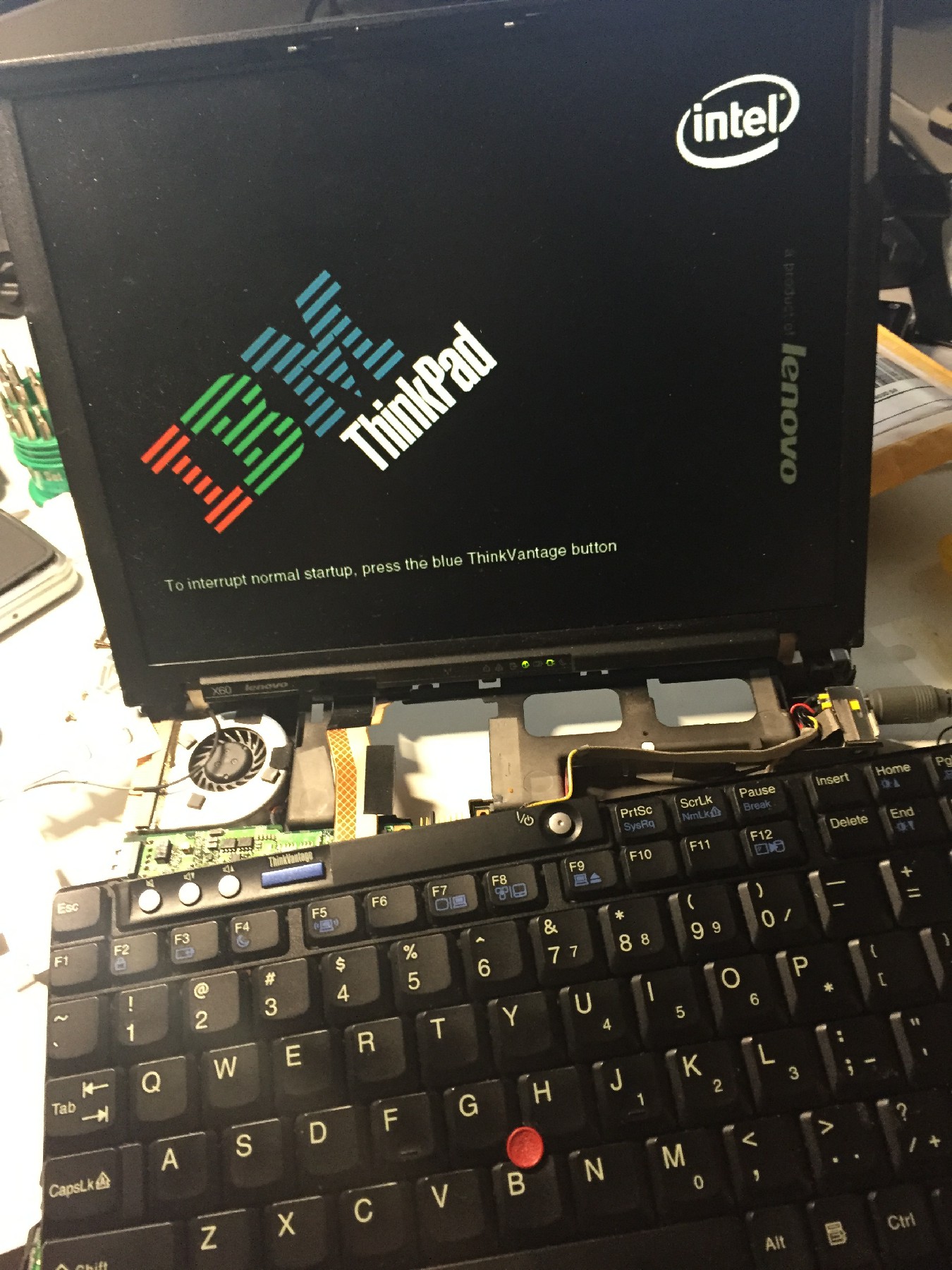
In the BIOS it should show you the new processor:
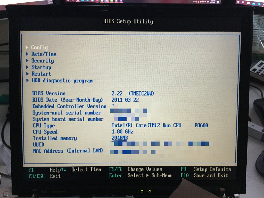
Ignore the speed shown in BIOS. In the operating system, CPU-Z should show you the processor is indeed running at 2.4GHz:
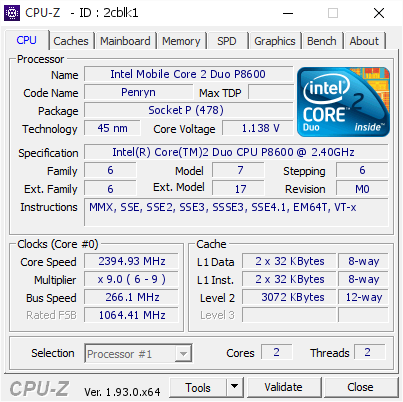
CPU-Z validation: http://valid.x86.fr/2cblk1
Final Words
So now I have an X61s with a Core 2 Duo P8600. I am glad everything worked. But do I recommend anyone doing this? Maybe not. Even T9900 or Q9100 should be considered as outdated in 2020. Modding this takes tons of time, a lot of money, and offers little in return (P8600 offers a nice 70% boost over the original L7500, but junk * 1.7 is still junk). This just finished off one of my dreams. I have been thinking about upgrading the CPU of my X61s for many years, but I simply wasn't confident enough to do this before. Thanks to everyone who shares their knowledge and experience online, without them this wouldn't be possible. Hope you enjoyed reading this, thanks for reading.