Specifications
- CPU:MCIMX6Y2DVM05AB(528MHz,Cortex A7)
- RAM:H5TQ2G63GFR(256MB,DDR3)
- Flash:H27U4G8F2D(512MB,3.3V)
- PMIC:PF1550
- LCD:GPM1006(320xRGBx240,Serial-RGB,ILI9322B)
- TSC:GT9288
Boot Mode
The following test points are present on the PCB:
- BT0L - Boot Mode 0 Low
- BT0H - Boot Mode 0 High
- BT1L - Boot Mode 1 Low
- BT1H - Boot Mode 1 High
Circuits nearby: (front side)
GND  T1H  T1H  GND
10K  10K   0R   NC
TMOD 3V3  T1L  T1L

GND  T0H  T0H  GND
4K7   NC   NC   NC
TCK  3V3  T0L  T1L
To enter USB DFU mode:
- Remove the 10K resistor between T1H and 3V3
- Solder a 10K resistor between T0H and 3V3
- Solder a 0R resistor between T0H and T0L (not sure if necessary)
There should be (lot of) other possible ways to change the bootmode or force it to fallback to the DFU mode.
Note: It is technically not a USB DFU (Device Firmware Upgrade) mode as it does not utilize the standard DFU protocol. It uses the i.MX Serial Download Protocol. I call it DFU as this is a more common term for such things.
Pin Assignments
| Pin | Default | Function | Verified |
|---|---|---|---|
| GPIO1_0 | 1 | ||
| GPIO1_1 | 1 | ||
| GPIO1_2 | 1 | led_green_n | y |
| GPIO1_3 | 0 | ||
| GPIO1_4 | 0 | ||
| GPIO1_5 | 0 | ||
| GPIO1_6 | 0 | ||
| GPIO1_7 | 1 | led_blue_n | y |
| GPIO1_8 | 1 | ||
| GPIO1_9 | 1 | led_red_n | y |
| GPIO1_10 | 0 | ||
| GPIO1_11 | 0 | ||
| GPIO1_12 | 0 | ||
| GPIO1_13 | 0 | ||
| GPIO1_14 | 0 | ||
| GPIO1_15 | 0 | ||
| GPIO1_16 | 0 | uart1_tx | y |
| GPIO1_17 | 0 | uart1_rx | y |
| GPIO1_18 | 0 | ||
| GPIO1_19 | 1 | ||
| GPIO1_20 | 1 | ||
| GPIO1_21 | 0 | ||
| GPIO1_22 | 0 | ||
| GPIO1_23 | 0 | ||
| GPIO1_24 | 0 | ctp_rst | y |
| GPIO1_25 | 0 | ctp_int | y |
| GPIO1_26 | 0 | ||
| GPIO1_27 | 0 | ||
| GPIO1_28 | 1 | i2c1_scl | y |
| GPIO1_29 | 1 | i2c1_sda | y |
| GPIO1_30 | 1 | i2c2_scl | n |
| GPIO1_31 | 1 | i2c2_sda | n |
| GPIO2_0 | 0 | ||
| GPIO2_1 | 0 | kpp_col0 | y |
| GPIO2_2 | 0 | kpp_row1 | y |
| GPIO2_3 | 0 | kpp_col1 | y |
| GPIO2_4 | 0 | kpp_row2 | y |
| GPIO2_5 | 0 | kpp_col2 | y |
| GPIO2_6 | 0 | kpp_row3 | y |
| GPIO2_7 | 0 | kpp_col3 | y |
| GPIO2_8 | 0 | kpp_row4 | y |
| GPIO2_9 | 0 | kpp_col4 | y |
| GPIO2_10 | 0 | kpp_row5 | y |
| GPIO2_11 | 0 | kpp_col5 | y |
| GPIO2_12 | 0 | kpp_row6 | y |
| GPIO2_13 | 0 | kpp_col6 | y |
| GPIO2_14 | 0 | kpp_row7 | y |
| GPIO2_15 | 0 | kpp_col7 | y |
| GPIO2_16 | 0 | ||
| GPIO2_17 | 0 | ||
| GPIO2_18 | 0 | ||
| GPIO2_19 | 0 | ||
| GPIO2_20 | 0 | ||
| GPIO2_21 | 0 | lcd_bl_bat_en | y |
| GPIO3_0 | 0 | lcd_clk | y |
| GPIO3_1 | 0 | lcd_enable | y |
| GPIO3_2 | 0 | lcd_hsync | y |
| GPIO3_3 | 0 | lcd_vsync | y |
| GPIO3_4 | 0 | lcd reset | y |
| GPIO3_5 | 0 | lcd_data0 | y |
| GPIO3_6 | 0 | lcd_data1 | y |
| GPIO3_7 | 0 | lcd_data2 | y |
| GPIO3_8 | 0 | lcd_data3 | y |
| GPIO3_9 | 0 | lcd_data4 | y |
| GPIO3_10 | 0 | lcd_data5 | y |
| GPIO3_11 | 0 | lcd_data6 | y |
| GPIO3_12 | 0 | lcd_data7 | y |
| GPIO3_13 | 0 | ||
| GPIO3_14 | 0 | ||
| GPIO3_15 | 0 | ||
| GPIO3_16 | 1 | ||
| GPIO3_17 | 0 | ||
| GPIO3_18 | 0 | ||
| GPIO3_19 | 0 | ||
| GPIO3_20 | 0 | ||
| GPIO3_21 | 0 | ||
| GPIO3_22 | 0 | ||
| GPIO3_23 | 0 | ||
| GPIO3_24 | 0 | ||
| GPIO3_25 | 0 | ||
| GPIO3_26 | 0 | ||
| GPIO3_27 | 0 | ||
| GPIO3_28 | 0 | ||
| GPIO4_0 | 1 | nand_re_b | n |
| GPIO4_1 | 1 | nand_we_b | n |
| GPIO4_2 | 0 | nand_data0 | n |
| GPIO4_3 | 0 | nand_data1 | n |
| GPIO4_4 | 0 | nand_data2 | n |
| GPIO4_5 | 0 | nand_data3 | n |
| GPIO4_6 | 0 | nand_data4 | n |
| GPIO4_7 | 0 | nand_data5 | n |
| GPIO4_8 | 0 | nand_data6 | n |
| GPIO4_9 | 0 | nand_data7 | n |
| GPIO4_10 | 0 | nand_ale | n |
| GPIO4_11 | 0 | nand_wp_b | n |
| GPIO4_12 | 1 | nand_ready_b | n |
| GPIO4_13 | 1 | nand_ce0_b | n |
| GPIO4_14 | 0 | nand_ce1_b | n |
| GPIO4_15 | 0 | nand_cle | n |
| GPIO4_16 | 0 | nand_dqs | n |
| GPIO4_17 | 0 | ||
| GPIO4_18 | 0 | ||
| GPIO4_19 | 0 | lcd backlight | y |
| GPIO4_20 | 0 | ||
| GPIO4_21 | 0 | lcd sck | y |
| GPIO4_22 | 0 | lcd cs | y |
| GPIO4_23 | 0 | lcd sda | y |
| GPIO4_24 | 1 | ||
| GPIO4_25 | 1 | ||
| GPIO4_26 | 0 | ||
| GPIO4_27 | 0 | ||
| GPIO4_28 | 0 | ||
| GPIO5_0 | 0 | ||
| GPIO5_1 | 0 | ||
| GPIO5_2 | 0 | ||
| GPIO5_3 | 0 | ||
| GPIO5_4 | 0 | ||
| GPIO5_5 | 0 | ||
| GPIO5_6 | 0 | ||
| GPIO5_7 | 0 | ||
| GPIO5_8 | 0 | ||
| GPIO5_9 | 0 | ||
| GPIO5_10 | 1 | ||
| GPIO5_11 | 0 |
Power Management
The power mangement is done by using one PF1550 PMIC, connected to I2C1. The I2C address is 0x08.
The LCD is powered by LDO1. The default voltage is 1.8V, and should be set to 3.3V for the LCD to function correctly.
RW the PMIC from U-boot:
i2c dev 0
i2c md 0x08 0x00 1
i2c mw 0x08 0x4c 0x1f 1
Currently unsure the connection of WDI and INTB.
Power key (ON) is connected to i.MX6's SNVS power key input. Currently unsure if it is also connected to PF1550's power key input.
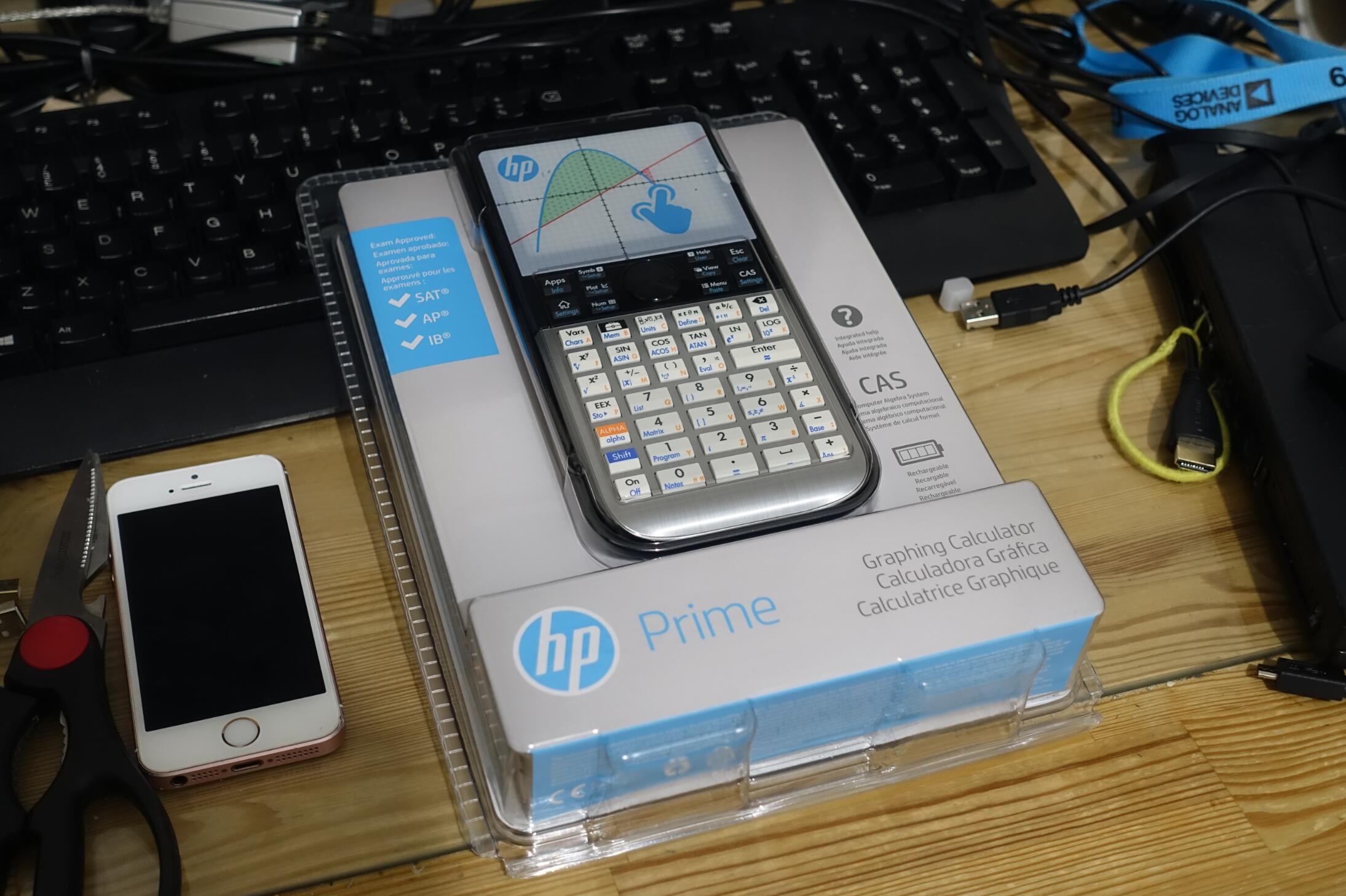
Keypad
| ROW1 | ROW2 | ROW3 | ROW4 | ROW5 | ROW6 | ROW7 | |
|---|---|---|---|---|---|---|---|
| COL0 | EEX | Bksp | +/- | Num | 9 | , | Enter |
| COL1 | 0 | xtθn | x^2 | Plot | CAS | 8 | Right |
| COL2 | / | Templ | LOG | Symb | Menu | 7 | |
| COL3 | * | ALPHA | LN | HOME | View | 6 | |
| COL4 | - | a b/c | TAN | APPS | Up | 5 | |
| COL5 | + | Vars | COS | Down | 1 | 4 | |
| COL6 | Space | SIN | Shift | Esc | . | 3 | |
| COL7 | Left | Tools | x^y | ( ) | Help | 2 |
- Tools: Toolbox key in the first row of main keyboard
- Templ: Template key in the first row of main keyboard
LCD
LCD backlight DCDC has two power sources, VBUS and VBAT. They are connected together using diodes. VBUS is always connected, and VBAT is controlled by GPIO2_21.
Backlight DCDC chip is an AME5142 equivalent.
CTP
I2C address 0x14, powered using LDO1 (shared with LCD). Linux kernel driver "goodix, gt928" seems to work fine.