Introduction
Dramite aims to build a small PC-compatible SBC based on an Intel 80386DX processor and an FPGA to emulate a custom chipset. There are several reasons why I am building a 386 PC in 2021:
- To learn Chisel
- I happen to have lots of 386DX chips lying around
- Just because
I expect this to be a long term project, and this is the first project log. I am trying not to explain too many details in these notes. This should not be a tutorial, but just some facts.
Overall Architecture
An FPGA is used as the bridge. It would handle everything from memory controller, floating point co-processor, to legacy IO bus, USB keyboard and mouse IO port emulation.
On a high level, the design would be simply connect the 386DX to the FPGA, done. However, it is still unclear how to approach everything in the FPGA. We could try to replicate things that exists on real 386 motherboards, such as direct connect between 386 and 387, SRAM caches, ISA buses, multiple devices attached to the ISA buses, etc. But this might not be the optimal solution, and sometimes may not even apply. For example, we would not have FPM/EDO RAMs on our board. Instead I would like to start from a performance perspective, looking at what we have, and see what would be the optimal architecture design.
Local Bus
The processor is the 386DX, I obviously couldn't modify the internals of the processor to enhance the performance. But I want to ensure I get the most out of it. The best I can do is to allow the bus access to finish as quick as possible (0 wait state).
The 386 also allows the bus to be pipelined, so it would sends the address one cycle eariler, to give the memory more time to access. Unfortunately this function also comes with a cost:
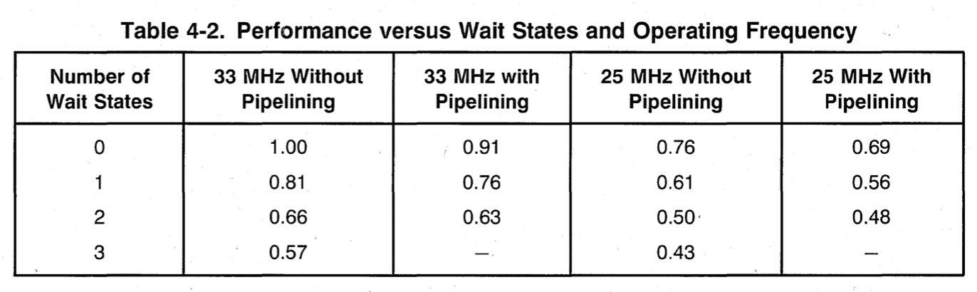
Table comes from Intel 80386DX Microprocessor Hardware Reference Manual. As you may see, by enabling the pipelining, we lose 9% of performance. This is still better than 1 wait state, which we loose 19% of performance. We shall see how these means in terms of the time for the FPGA to respond.
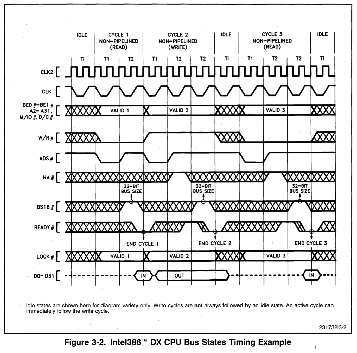
In the non-pipelined case, looking at CYCLE 1, the 386DX outputs the valid address and control signals on the falling edge of CLK in T1. Means the FPGA could latch the data in on the rising edge of CLK in T1. The 386DX expects the data to be ready on the falling edge of CLK in T2, means the FPGA should put out the data on the rising edge of CLK in T2. The FPGA has exactly one cycle time in CLK to prepare the data. CLK runs at 33MHz, translates to a cycle time of 30ns. The whole bus cycle lasts for 60ns, and FPGA has 30ns to prepare the data.
If one wait state is added, such as in CYCLE 3, the whole cycle is now 90ns. And the FPGA has 60ns to prepare the data in this case.
What about pipelined?
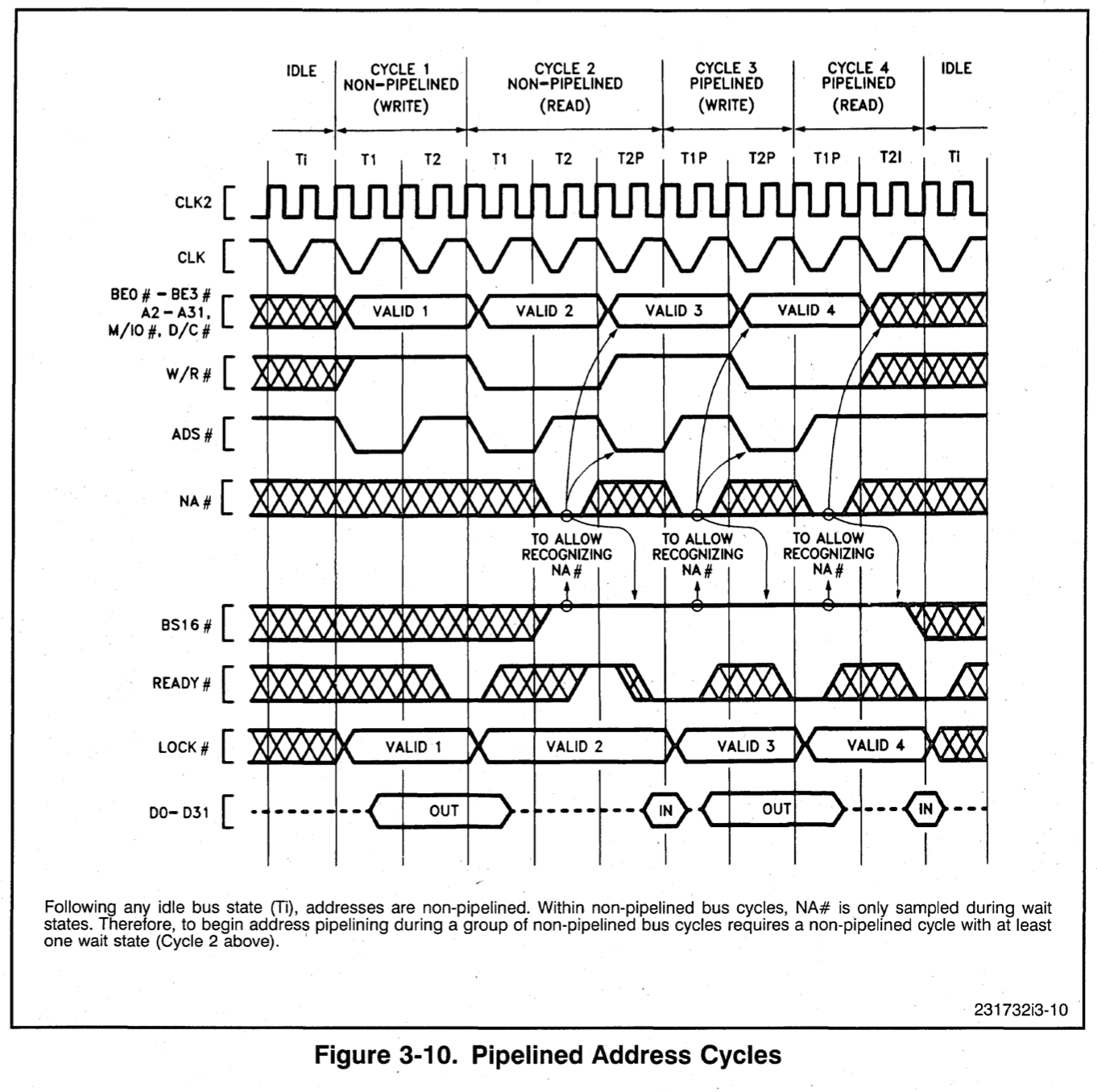
The bus cycle time is still 60ns, but the FPGA now gets 60ns to prepare the data. Remember this is with 9% of performance penalty.
In conclusion, to achieve the absolutely best performance, we use non-pipelined mode and supply the data in single cycle. It is currently unknown if it would provide any performance improvement if I mix both modes.
Cache
Obviously, some form of cache is needed to provide the data in 30ns. But what kind of?
The on-chip memory of FPGA would certainly be fast enough to provide data in 30ns.
Off-chip high speed SRAMs would also be able to provide data in 30ns. We could use the normal SRAM chips to build the cache if we want, at the cost of layout complexity and IO pin usage.
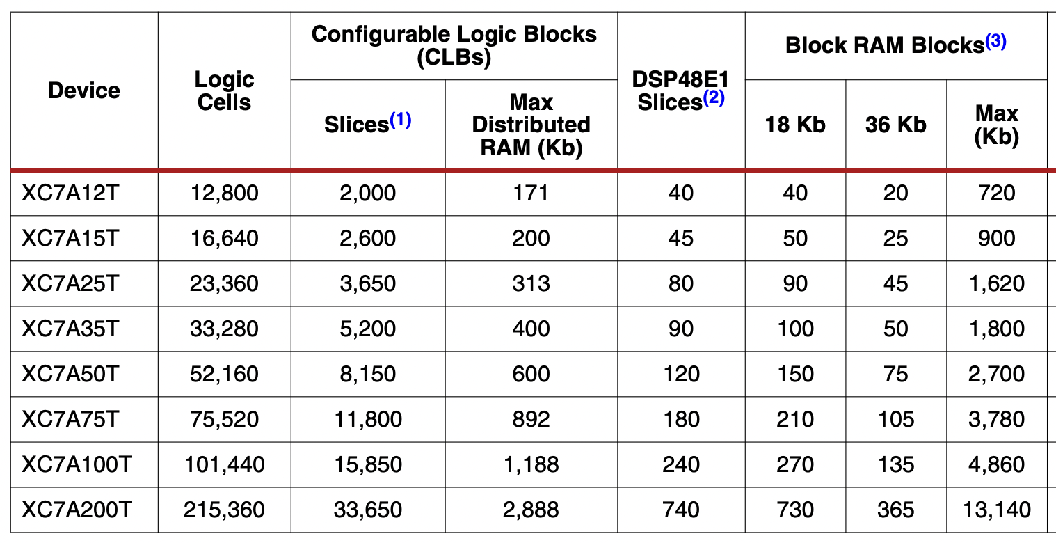
FPGA on-chip memory size, just for reference.
DRAM
How slow is the DRAM?
Using the DDR3 MIG on Aritx-7, with AXI interface, we could see the typical read latency:
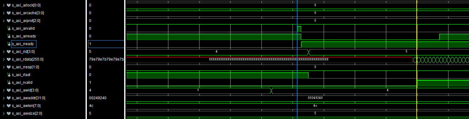
The time difference is 63799.5ns - 63607.5ns = 192ns.
But if we think the DRAM controller is probably not very optimized, what's is the time it takes the DDR3 memory itself to read the data?
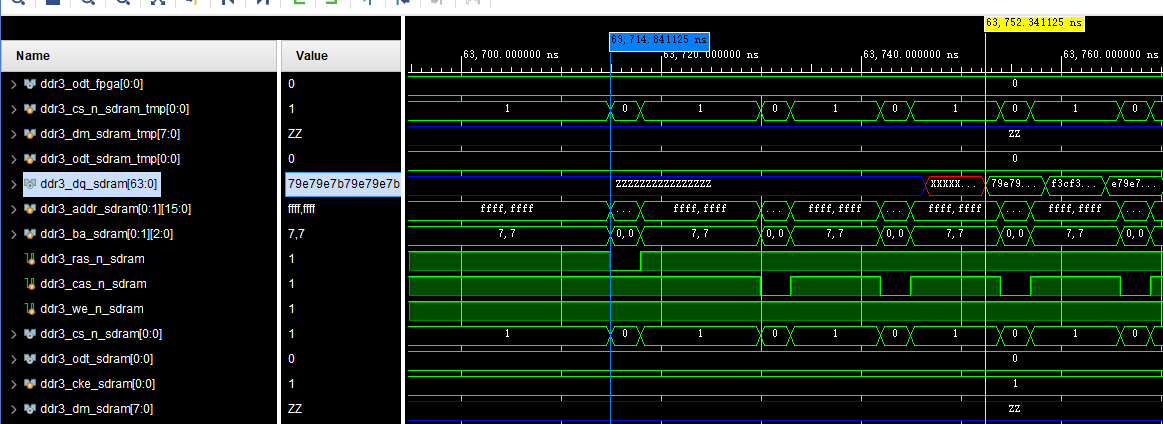
Much faster. 63746ns - 63714ns = 32ns, just a little above the cycle time that 386 would take.
But the cache is still needed. It is just the cache miss penalty wouldn't be too bad.
Hardware IO Planning
- 80386DX: 79 5V IOs (with address pipeline mode disabled, 32 bit only, no bus take-over)
- RGMII: 16 1.5V/1.8V/2.5V/3.3V IOs
- Audio: 3 1.8V/3.3V IOs
- USB ULPI: 11 1.8V/3.3V IOs + 1 RESET (could be open-drain)
- SDIO: 6 3.3V IOs
- HDMI: 4 TMDS pairs (GTP + voltage translator, or 3.3V IO)
- DDR3 SODIMM: 118 1.5V IOs
The 80386DX needs voltage translator, and best 3.3V-5V for minimal propagation delay. Plus 1 direction control pin for databus, so that's 80 3.3V IOs. Basically means 2 of the IO banks needs to be 3.3V.
The DDR3 uses 3 IO banks, so 3 of the IO banks needs to be 1.5V.
And some common I2C control channels for audio, SPD, HDMI, etc. Count as 4, any voltage.
XC7A35T has 6 available IO banks:
- IO Bank 14: 50 IOs, 1.5V
- IO Bank 15: 50 IOs, 1.5V
- IO Bank 16: 50 IOs, 1.5V
- IO Bank 34: 50 IOs, 3.3V
- IO Bank 35: 50 IOs, 3.3V
- IO Bank 216: 4 TX pairs and 4 RX pairs
In total it has 150 1.5V IOs, 100 3.3V IOs, 4 TX pairs, and 4 RX pairs.
In total 134+5 1.5 IOs, 100 3.3 IOs, 4 TX pairs needed. It still has 11 1.5V IOs and 4 RX pairs left.